Are the JTAG ports of JH7110 available on visionfive 2? Seems they are not on 40-pin gpio port.
The area probably in the 40 pin header. They’re hard to find because there is a huge pin multiplexer that can be manipulated by code running before your code that can move them.
I haven’t successfully sussed them out yet on Pine64,. Though we did succeed (and build boards for) BeagleV.
Someone (dramforever?) Has a good blog post on this, but I don’t remember what board. It was while I was between JH parts.
Thanks. I’ll try when I get the board.
I have configured some pinmux in dts and tried to connect the chip with jlink.
I got these error. Is the jlink not support the chip or other config issue ?
ConfigTargetSettings() start
ConfigTargetSettings() end
TotalIRLen = 10, IRPrint = 0x0021
JTAG chain detection found 2 devices:
#0 Id: 0x07110CFD, IRLen: 05, Unknown device
#1 Id: 0x07110CFD, IRLen: 05, Unknown device
Connect failed. Resetting via Reset pin and trying again.
Interesting that you see two and not four 7110’s.
You mention Segger’s Jlink. YOu may have to manually tell it which tap to use via their scripting tools, ala Manual setup of JTAG chain - SEGGER Wiki
StarFive Official U-boot has been configured the JTAG port. Can be found here → u-boot/starfive_visionfive2.c at JH7110_VisionFive2_devel · starfive-tech/u-boot · GitHub
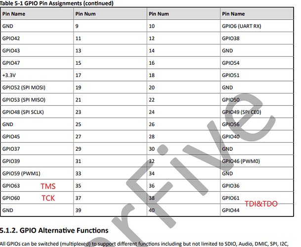
Corresponding to the 40pin header, as shown in the figure below
Using the jlink to connect the chip, can refer to J-Link RISC-V - SEGGER Wiki
int InitTarget(void) {
  //
  // TDI -> TAP_#1 -> TAP_#0 -> TDO
  //
  // TAP_#0 info:
  //   IRLen: 5
  //   TAPId: 0xDEB11001
  //
  // TAP_#1 info:
  //   IRLen: 5
  //   TAPId: 0x20000913
  //
  //
  // Code to connect to TAP_#1
  //
  JLINK_JTAG_DRPre  = 1;
  JLINK_JTAG_DRPost = 0;
  JLINK_JTAG_IRPre  = 5;
  JLINK_JTAG_IRPost = 0;
  JLINK_JTAG_IRLen  = 5;
  JLINK_JTAG_SetDeviceId(0, 0xDEB11001);
  JLINK_JTAG_SetDeviceId(1, 0x20000913);
  return 0;
}
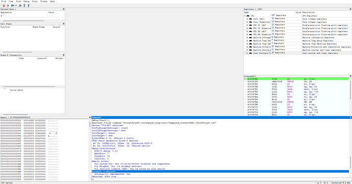
Ozone with Jlink-v11 on tap1 like this:
No need to use SetDeviceId function. Previous config+Selection of U74-MC is enough.
Besides, that device id(0xDEB11001) is actually Syntacore’s device ID, not Sifive.
I’m using this:
int InitTarget(void) {
  //
  // TDI -> TAP_#1 -> TAP_#0 -> TDO
  //
  // TAP_#0 info:
  //   Maybe E24?
  //   IRLen: 5
  //
  // TAP_#1 info:
  //   U74-MC here
  //   IRLen: 5
  //
  //
  // Code to connect to TAP_#1
  //
  JLINK_JTAG_DRPre  = 1;
  JLINK_JTAG_DRPost = 0;
  JLINK_JTAG_IRPre  = 5;
  JLINK_JTAG_IRPost = 0;
  JLINK_JTAG_IRLen  = 5;
  JLINK_SetDevice("U74-MC");
  return 0;
}
I noticed a problem when selecting harts.
Script here:
int InitTarget(void)
{
  //
  // TDI -> TAP_#1 -> TAP_#0 -> TDO
  //
  // TAP_#0 info:
  //   Maybe E24?
  //   IRLen: 5
  //
  // TAP_#1 info:
  //   U74-MC here
  //   IRLen: 5
  //
  //
  // Code to connect to TAP_#1
  //
  JLINK_JTAG_DRPre  = 1;
  JLINK_JTAG_DRPost = 0;
  JLINK_JTAG_IRPre  = 5;
  JLINK_JTAG_IRPost = 0;
  JLINK_JTAG_IRLen  = 5;
  JLINK_SetDevice("U74-MC");
  return 0;
}


// Select needed hart
// Seems Jlink could not handle multi-core debugging at the same time through script file?
// Or there exists some APIs not written in official wiki that could handle this?
int SetupTarget(void)
{
  int ret;

  U32 dmcontrol_addr;

  U32 hasel_mask;
  U32 hartsello_mask;
  U32 hartselhi_mask;

  U32 dmcontrol_value;
  U32 hart_id;
  U32 hart_id_target;

  // Set wanted hart id here(0 is S7 core, 1~4 is U74 core)
  hart_id = 3;

  ret = 0;
  dmcontrol_addr = 0x10;
  hasel_mask = 0x04000000;
  hartsello_mask = 0x03FF0000;
  hartselhi_mask = 0x0000FFC0;

  // Core selection through writing DMI registers

  // First, do automatic configure
  // Needed or connection would fail
  ret = JLINK_RISCV_DMI_AutodetectDMISettings();
  if(ret < 0)
  {
    return ret;
  }

  // Second, read dmcontrol to get current hart;
  ret = JLINK_RISCV_DMI_ReadReg(dmcontrol_addr, &dmcontrol_value);
  if(ret < 0)
  {
    return ret;
  }
  hart_id_target = ((dmcontrol_value & hartsello_mask) >> 16) | ((dmcontrol_value & hartselhi_mask) << 4);
  JLINK_SYS_Report("********************************");
  JLINK_SYS_Report("Pre-selection info");
  JLINK_SYS_Report1("dmcontrol value is: ", dmcontrol_value);
  JLINK_SYS_Report1("Current hart id is: ", hart_id_target);
  JLINK_SYS_Report("********************************");

  // Third, modify dmcontrol value to select wanted hart.
  dmcontrol_value = dmcontrol_value | ((hart_id & (hartsello_mask >> 16)) << 16) | ((hart_id & (hartselhi_mask << 4)) >> 4);
  ret = JLINK_RISCV_DMI_WriteReg(dmcontrol_addr, dmcontrol_value);
  if(ret < 0)
  {
    return ret;
  }

  // Fourth, check if configure is successful
  ret = JLINK_RISCV_DMI_ReadReg(dmcontrol_addr, &dmcontrol_value);
  hart_id_target = ((dmcontrol_value & hartsello_mask) >> 16) | ((dmcontrol_value & hartselhi_mask) << 4);
  JLINK_SYS_Report("********************************");
  JLINK_SYS_Report("Post-selection info");
  JLINK_SYS_Report1("dmcontrol value is: ", dmcontrol_value);
  JLINK_SYS_Report1("Current hart id is: ", hart_id_target);
  JLINK_SYS_Report("********************************");

  return ret;
}
However, reading mhartid and misa always reports using hart 0(S76).
SEGGER J-Link Commander V7.86h (Compiled Apr 12 2023 16:11:59)
DLL version V7.86h, compiled Apr 12 2023 16:10:23

Connecting to J-Link via USB...O.K.
Firmware: J-Link V11 compiled Mar 28 2023 16:59:55
Hardware version: V11.00
J-Link uptime (since boot): 0d 00h 06m 32s
S/N: 261011862
License(s): FlashBP, GDB
OEM: SEGGER-EDU
USB speed mode: High speed (480 MBit/s)
VTref=3.300V (fixed)


Type "connect" to establish a target connection, '?' for help
J-Link>connect
Please specify device / core. <Default>: U74-MC
Type '?' for selection dialog
Device>
Please specify target interface:
  J) JTAG (Default)
  S) SWD
  T) cJTAG
TIF>
Device position in JTAG chain (IRPre,DRPre) <Default>: -1,-1 => Auto-detect
JTAGConf>
Specify target interface speed [kHz]. <Default>: 4000 kHz
Speed>15000
Device "U74-MC" selected.


Connecting to target via JTAG
ConfigTargetSettings() start
ConfigTargetSettings() end - Took 6us
InitTarget() start
Device "U74-MC" selected.
InitTarget() end - Took 1.15ms
TotalIRLen = 10, IRPrint = 0x0021
JTAG chain detection found 2 devices:
 #0 Id: 0x07110CFD, IRLen: 05, Unknown device
 #1 Id: 0x07110CFD, IRLen: 05, Unknown device
Debug architecture:
  RISC-V debug: 0.13
  AddrBits: 7
  DataBits: 32
  IdleClks: 5
Memory access:
  Via system bus: Yes (8/16/32/64-bit accesses are supported)
  Via ProgBuf: Yes (16 ProgBuf entries)
  Via abstract command (AAM): May be tried as last resort
DataBuf: 2 entries
  autoexec[0] implemented: Yes
Detected: RV64 core
Temp. halting CPU for for feature detection...
HW instruction/data BPs: 8
Support set/clr BPs while running: No
HW data BPs trigger before execution of inst
CSR access via abs. commands: No
Feature detection done. Restarting core...
BG memory access support: Via SBA
SetupTarget() start
********************************
Pre-selection info
dmcontrol value is: 0x00000001
Current hart id is: 0x00000000
********************************
********************************
Post-selection info
dmcontrol value is: 0x00030001
Current hart id is: 0x00000003
********************************
SetupTarget() end - Took 3.56ms
Memory zones:
  Zone: "Default" Description: Default access mode
RISC-V identified.
J-Link>halt
pc = 000000004000AB9A sp = 0000000040060F00 ra = 000000004000ABA0
gp = 0000000000000000 tp = 0000000040061000 fp = 0000000040060F30
t0 = 0000000000000022 t1 = 0000000000000000 t2 = 0000000000000000
t3 = 0000000000000000 t4 = 0000000000000000 t5 = 0000000000000000 t6 = 0000000000000000
a0 = 0000000000000001 a1 = 0000000000000000 a2 = 0000000000000000 a3 = 0000000000090006
a4 = 0000000002000000 a5 = 0000000000000808 a6 = 0000000000000000 a7 = 0000000000000000
s1 = 0000000040061068 s2 = 0000000000000002 s3 = 0000000000000000 s4 = 0000000040042000
s5 = 0000000040042020 s6 = 0000000000000000 s7 = 0000000000000018 s8 = 0000000000002000
s9 = 000000004004EAB8 s10 = 0000000000000000 s11 = 0000000000000000
J-Link>readcsr 0xF11
CSR 0x0F11: 0x00000489
J-Link>readcsr 0xF12
CSR 0x0F12: 0x8000000000000007
J-Link>readcsr 0xF13
CSR 0x0F13: 0x04210427
J-Link>readcsr 0xF14
CSR 0x0F14: 0x00000000
J-Link>readcsr 0x301
CSR 0x0301: 0x8000000000901107
Did anyone get jag working properly?
I built a custom patched version of upstream u-boot to enable jtag in spl. It works with openocd, but as soon as I jump into opensbi it breaks. I guess the jtag does not like it when the board executes from ram?
I also patched spl to load directly from memory, this way I do not need to reflash sd card, but can load the stage2 via the jtag into ram. It seems to work, but when the spl finally jumps into ram it also stops working.
If anyone knows if I have to do something special to get jtag debugging working, when executing from ram, I would appreciate it.
Maybe opensbi resets the pinmux?
Nope, it can still talk to the internal jtag ports. Only the debug module of one of the cores stops working.
I got it working now, but it seems there might be a some kind of bug in the chip.
When you have a breakpoint, or stop a core when it has just jumped to dram, it will hang the debug module, core and generally everything associated to that CPU.
I tried to recover the debug module with now connected nTRST, but it did not help. Only a hard board reset helps.
If you stop it after some instructions were already executed in sdram, it fixes the problem.
I do not think its the fault of software. If I step instruction by instruction it literally hangs every time I jump directly from sram to dram.
I got the same problem as @ruabmbua mentioned.
I followed a guide from below link
However, I failed to jump 0x40000000 where OpenSBI is located.
Error: Timed out after 2s waiting for busy to go low (abstractcs=0x10001002). Increase the timeout with riscv set_command_timeout_sec.
Warn : Failed to read memory via program buffer.
Seems like SPL is booted the S7 core but the openocd script only provides a connection to u74 cores. Anyway, did anyone who can successfuly jump into opensbi using JTAG from spl?
I did it. But as mentioned you need to avoid single stepping directly into sdram / opensbi. Also setting a breakpoint at entry will break it. I set a breakpoint to a init function in opensbi that is a couple instructions after entry, then it worked.
Can you descriptor more details?
From cross-referencing the uboot source, the preliminary TRM: reference header, and the pinout diagram the JTAG pinout is:
- RST(4): Pin 36, GPIO36
- TDI(19): Pin 38, GPIO61
- TDO(8,22): Pin 40, GPIO44
- TMS(20): Pin 35, GPIO63
- TCK(29): Pin 37, GPIO60
The number in parentheses is the signal number assigned in the reference header. Hope this helps ![]()
If looking at the board with the GPIO pins on the right, the last three pins on the right should be filled, and the third-to-last and second-to-last pins on the left should be filled (leaving the last pin GND on the left open).
Edit: I would post a link to the pinout diagram, but I’m only allowed two links for now. It’s the one that comes up on RV space when searching “VisionFive2 pinout diagram”.
Basically, the same information @riturbo posted, with the added RST pin. Not sure if this is what you were asking for more details about.


